1 上海理工大学 光子芯片研究院,上海 200093
2 上海理工大学 光电信息与计算机工程学院,上海 200093
二维材料具有高折射率和高透光率等优异光学特性,利用激光加工氧化石墨烯材料,会发生还原反应并生成具有类石墨烯材料特性的还原氧化石墨烯,这使得基于氧化石墨烯材料设计菲涅耳透镜成为可能。相较于传统的光学透镜及微型光学透镜,这一设计将透镜的尺寸从厘米级缩减到纳米级。针对工作波长532 nm设计了基于氧化石墨烯薄膜的菲涅耳透镜,通过瑞利–索末菲衍射理论及电磁场数值仿真测试了菲涅耳透镜的聚焦效果,并且通过滴铸法制备了氧化石墨烯薄膜(约500 nm),在薄膜上用激光加工菲涅耳透镜,最终得到透镜聚焦光斑直径2.14 μm,聚焦效率41.2%。相比旋涂法制备氧化石墨烯薄膜,滴铸法制备氧化石墨烯具有效率高、价格低廉的优点。该设计为纳米级的基于氧化石墨烯的光学系统的集成化和大规模生产提供了可能。
氧化石墨烯 菲涅耳透镜 激光加工 还原氧化石墨烯 graphene oxide Fresnel lens laser processing reduced graphene oxide
1 上海理工大学光子芯片研究院,上海 200093
2 上海理工大学光电信息与计算机工程学院,上海 200093
近年来,受生物神经系统结构和功能的启发,神经形态计算引起广泛兴趣。忆阻器可以通过其电荷或磁通量调节电导,与人脑突触作用机制相似,是神经形态计算最有前途的候选器件之一。提出一种基于飞秒激光加工氧化石墨烯基忆阻器的方法,通过调整器件两端扫描电压,实现了极性可控的电阻开关:低电压下,器件表现出单极性电阻开关特性,在150个循环扫描中呈现高度稳定性,且功耗仅有0.75 nW;高电压下,器件呈现双极性开关特性。伴随测试次数的增加,器件整体电导逐步增加,同时分别讨论了两种电压下器件的开关机制。
极性可控 激光加工 氧化石墨烯 忆阻器 激光与光电子学进展
2024, 61(3): 0323002
Author Affiliations
Abstract
1 Institute of Photonic Chips, University of Shanghai for Science and Technology, Shanghai 200093, China
2 School of Optical-Electrical and Computer Engineering, University of Shanghai for Science and Technology, Shanghai 200093, China
3 Nokia Shanghai Bell Co., Ltd., Shanghai 201206, China
4 College of Medical Instruments, Shanghai University of Medicine and Health Sciences, Shanghai 201318, China
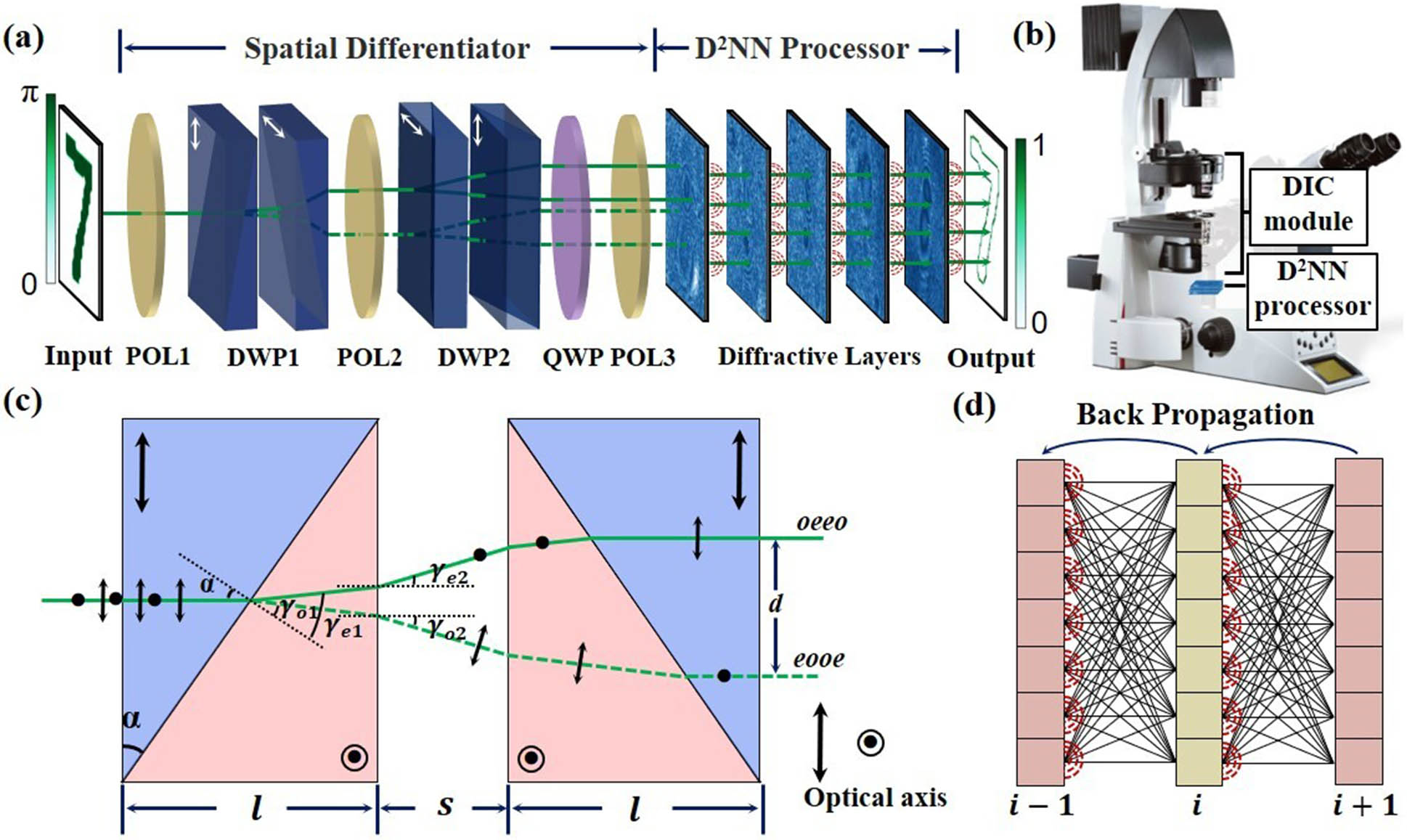
Edge detection for low-contrast phase objects cannot be performed directly by the spatial difference of intensity distribution. In this work, an all-optical diffractive neural network (DPENet) based on the differential interference contrast principle to detect the edges of phase objects in an all-optical manner is proposed. Edge information is encoded into an interference light field by dual Wollaston prisms without lenses and light-speed processed by the diffractive neural network to obtain the scale-adjustable edges. Simulation results show that DPENet achieves F-scores of 0.9308 (MNIST) and 0.9352 (NIST) and enables real-time edge detection of biological cells, achieving an F-score of 0.7462.
diffractive neural network edge detection phase objects Chinese Optics Letters
2024, 22(1): 011102
Author Affiliations
Abstract
1 Institute of Photonic Chips, University of Shanghai for Science and Technology, Shanghai 200093, China
2 Centre for Artificial-Intelligence Nanophotonics, School of Optical-Electrical and Computer Engineering, University of Shanghai for Science and Technology, Shanghai 200093, China
3 Key Laboratory of Optoelectronic Technology, Ministry of Education, Beijing University of Technology Beijing, China
The rapid development of neuromorphic computing has stimulated extensive research interest in artificial synapses. Optoelectronic artificial synapses using laser beams as stimulus signals have the advantages of broadband, fast response, and low crosstalk. However, the optoelectronic synapses usually exhibit short memory duration due to the low lifetime of the photo-generated carriers. It greatly limits the mimicking of human perceptual learning, which is a common phenomenon in sensory interactions with the environment and practices of specific sensory tasks. Herein, a heterostructure optoelectronic synapse based on graphene nanowalls and CsPbBr3 quantum dots was fabricated. The graphene/CsPbBr3 heterojunction and the natural middle energy band in graphene nanowalls extend the carrier lifetime. Therefore, a long half-life period of photocurrent decay - 35.59 s has been achieved. Moreover, the long-term optoelectronic response can be controlled by the adjustment of numbers, powers, wavelengths, and frequencies of the laser pulses. Next, an artificial neural network consisting of a 28 × 28 synaptic array was established. It can be used to mimic a typical characteristic of human perceptual learning that the ability of sensory systems is enhanced through a learning experience. The learning behavior of image recognition can be tuned based on the photocurrent response control. The accuracy of image recognition keeps above 80% even under a low-frequency learning process. We also verify that less time is required to regain the lost sensory ability that has been previously learned. This approach paves the way toward high-performance intelligent devices with controllable learning of visual perception.

Author Affiliations
Abstract
1 University of Shanghai for Science and Technology, Institute of Photonic Chips, Shanghai, China
2 University of Shanghai for Science and Technology, School of Optical-Electrical and Computer Engineering, Centre for Artificial-Intelligence Nanophotonics, Shanghai, China
The creation of biomimetic neuron interfaces (BNIs) has become imperative for different research fields from neural science to artificial intelligence. BNIs are two-dimensional or three-dimensional (3D) artificial interfaces mimicking the geometrical and functional characteristics of biological neural networks to rebuild, understand, and improve neuronal functions. The study of BNI holds the key for curing neuron disorder diseases and creating innovative artificial neural networks (ANNs). To achieve these goals, 3D direct laser writing (DLW) has proven to be a powerful method for BNI with complex geometries. However, the need for scaled-up, high speed fabrication of BNI demands the integration of DLW techniques with ANNs. ANNs, computing algorithms inspired by biological neurons, have shown their unprecedented ability to improve efficiency in data processing. The integration of ANNs and DLW techniques promises an innovative pathway for efficient fabrication of large-scale BNI and can also inspire the design and optimization of novel BNI for ANNs. This perspective reviews advances in DLW of BNI and discusses the role of ANNs in the design and fabrication of BNI.
direct laser writing neuron interface neural tissue engineering artificial neural networks Advanced Photonics
2022, 4(3): 034002
1 上海理工大学光子芯片研究院, 上海 200093
2 上海理工大学光电信息与计算机工程学院人工智能纳米光子学中心, 上海 200093
人工智能技术,特别是人工神经网络的创新引领了许多领域的应用革命,如网络搜索、计算机识别和语言、图像的识别技术。近年来纳米光子学的发展为传统的人工神经网络技术,特别是光学神经网络的发展带来了全新的物理视角以及截然不同的实现方法。一方面,纳米光子学是一门研究光与材料在纳米尺度相互作用的科学,可以带来全新的技术,如超分辨光学加工技术和超分辨光学成像技术,进而推动微纳尺度上多种功能的光学神经网络的实现。另一方面,纳米光子学中光子传播的多频段、高速度、低功耗的特点,促使了光学神经网络向着小体积、高密度、低功耗的方向发展。人工神经网络自身的发展也促使神经网络算法(如逆向设计、深度学习)在纳米光子学器件的设计中发挥前所未有的作用,以满足纳米光子学器件对自身功能、体积、集成度、计算功能的日益增长的要求。以神经网络的发展为起点,阐述人工神经网络特别是光学神经网络的发展趋势,以及人工神经网络与纳米光子学相互促进的发展历程。
光学器件 人工智能 人工神经网络 光学神经网络 纳米光子学 光学人工智能
Author Affiliations
Abstract
1 Laboratory of Artificial-Intelligence Nanophotonics, School of Science, RMIT University, Melbourne, Victoria 3001, Australia
2 Centre for Artificial-Intelligence Nanophotonics, School of Optical-Electrical and Computer Engineering, University of Shanghai for Science and Technology, Shanghai 200093, China
Neuromorphic computing applies concepts extracted from neuroscience to develop devices shaped like neural systems and achieve brain-like capacity and efficiency. In this way, neuromorphic machines, able to learn from the surrounding environment to deduce abstract concepts and to make decisions, promise to start a technological revolution transforming our society and our life. Current electronic implementations of neuromorphic architectures are still far from competing with their biological counterparts in terms of real-time information-processing capabilities, packing density and energy efficiency. A solution to this impasse is represented by the application of photonic principles to the neuromorphic domain creating in this way the field of neuromorphic photonics. This new field combines the advantages of photonics and neuromorphic architectures to build systems with high efficiency, high interconnectivity and high information density, and paves the way to ultrafast, power efficient and low cost and complex signal processing. In this Perspective, we review the rapid development of the neuromorphic computing field both in the electronic and in the photonic domain focusing on the role and the applications of memristors. We discuss the need and the possibility to conceive a photonic memristor and we offer a positive outlook on the challenges and opportunities for the ambitious goal of realising the next generation of full-optical neuromorphic hardware.
Author Affiliations
Abstract
Centre for Micro-Photonics, Faculty of Engineering and Industrial Sciences, Swinburne University of Technology, Hawthorn VIC 3122, Australia
We demonstrate the confinement of broadband optical energy in the visible to near-infrared regime in a threedimensional nanoscale volume with high energy efficiency in a nanostructure consisting of multiple nanoslits in dielectric chacolgenide material. We find that a broadband optical field can be confined down to the scale of 1 nm (λ∕650) with a confinement volume of λ3∕3 × 10<参考文献原文>The figure of merit of the nanostructure can be up to 10 times that achieved by plasmonic lensing and nanofocusing. Our work opens a new way for truly nanoscaled photonics applicable to nanolithograpy, nanoimaging, lab-on-chip nanosensing, single-molecule detection, and nanospectroscopy.
Subwavelength structures nanostructures Nanophotonics and photonic crystals Photonics Research
2013, 1(3): 03000136


